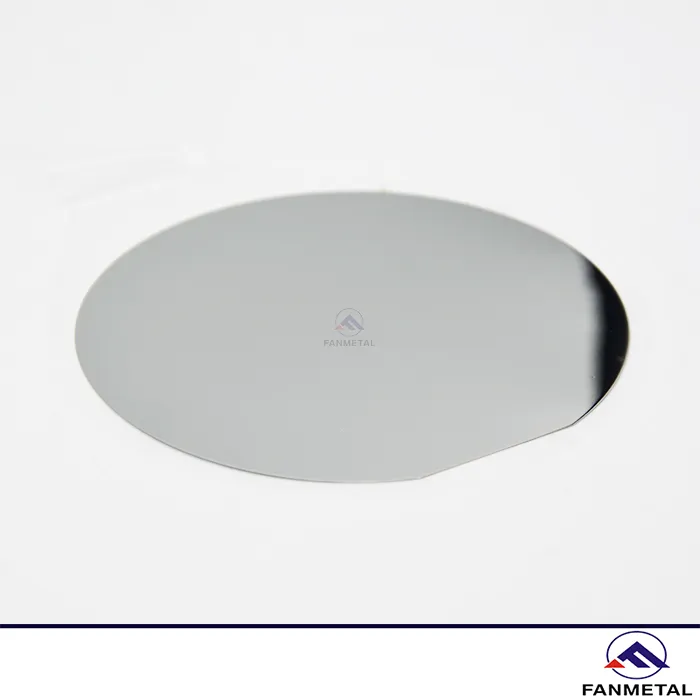

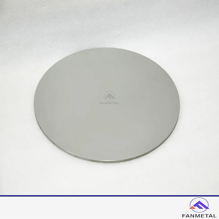
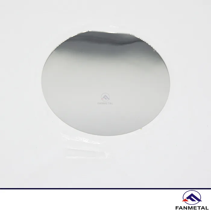
Molybdenum Semiconductor Wafers
Purity:≥99.95%
Size:5-300mm
Density:10.2 g/cm³
Thickness:0.1-5mm
Surface:Polished,Ra ≤ 0.8 μm
Melting Point:2617℃
Resistivity:5.2 μΩ·cm
Standard:ASTM B386
Delivery Time:25-30 DAYS
Certification:ISO 9001
Send Inquiry
Product Details ofMolybdenum Semiconductor Wafers
Overview
Molybdenum Semiconductor Wafers are high-performance, heat-resistant circular thin plates with diameters ranging from 2 inches to 8 inches (50.8 mm to 203.2 mm) and thicknesses greater than 0.05 mm. Molybdenum wafers have excellent electrical and thermal conductivity, high melting points, low thermal expansion coefficients, resistance to high-temperature creep, oxidation, and corrosion, and are widely used in semiconductors, power devices, optoelectronics, and high-temperature equipment. FANMETAL is a very trustworthy non-ferrous metal supplier with many years of production experience, and also produces other metal products such as molybdenum bars and molybdenum alloys.
Characteristics
Molybdenum wafers have a stable chemical composition, with molybdenum content up to 99.9%, precise dimensions, and low surface roughness (Ra < 1.6 μm). The main features of molybdenum wafers include:
- High temperature resistance: The melting point of molybdenum wafers is about 2623°C, making them less likely to deform or soften in high-temperature environments.
- Low coefficient of thermal expansion: The thermal expansion coefficient of molybdenum wafers is 4.8X10⁻⁶/K, which is close to silicon (2.6-4.0X10⁻⁶/K) and silicon carbide (4.0X10⁻⁶/K), effectively reducing thermal stress.
- Excellent thermal and electrical conductivity: Molybdenum wafers offer high heat dissipation efficiency and low resistivity, making them well-suited for high-power applications.
- High purity, low volatility: few impurities, low volatilization under high-temperature vacuum, no process contamination.
- Corrosion resistance and stability: resistant to acids, alkalis, and chemical corrosion, with a long service life.
- High precision: flat surface and precise dimensions meet precision machining requirements.
application
Molybdenum Wafers, with four core advantages-high melting point, low expansion, high thermal conductivity, and high purity stability-are widely used in the following application areas:
- Power semiconductor devices: Compatible with IGBT modules and high-power thyristors, Molybdenum Discs serve as heat dissipation substrates and contact electrodes, resisting thermal stress from hot and cold cycling and preventing chip damage. They are widely used in high-speed rail, smart grids, and industrial inverters.
- Third-generation semiconductors: Molybdenum wafers serve as heat dissipation substrates for SiC and GaN devices, offering excellent thermal expansion coefficients and stable operation in high-power scenarios such as new energy vehicles and 5G base stations.
- High-frequency RF devices: RF/microwave transistors used in satellite communications and military radar, serving as rigid grounding substrates, resistant to deformation, and ensuring precise high-frequency signal transmission.
- Semiconductor process tooling: High-purity Molybdenum carrier wafers are used to manufacture carrier disks for CVD, PVD, high-temperature annealing, and other processes, offering high flatness at high temperatures, free of impurity contamination, and suitable for chip manufacturing processes.
- Optoelectronic devices: Molybdenum Wafers, as precision heat sinks for high-power LEDs and laser diodes, quickly dissipate heat, eliminate hot spots, and improve device efficiency and lifespan.
Pure Molybdenum vs. TZM Molybdenum Alloy Wafers: How to Choose?
For extremely high-power laser LEDs (Laser Diodes), ordinary pure molybdenum may not be sufficient; in such cases, TZM Molybdenum Alloy Wafer is an even better upgrade option. TZM is the main alloy of molybdenum, composed of titanium, zirconium, and carbon. TZM is stronger than pure molybdenum, able to withstand temperatures exceeding 1300°C, and offers better weldability and overall strength.
Comparison table of horizontal parameters of pure molybdenum VS TZM
|
Physical and commercial characteristics |
Pure Molybdenum Alloy Wafers |
TZM Molybdenum Alloy Wafers |
|
Main ingredients |
≥95.95%Mo |
~99.3%Mo+0.5%Ti+0.08%Zr |
|
recrystallization temperature |
900℃-1000℃ |
1400℃ |
|
Maximum recommended operating temperature |
~1100℃ |
~1700℃ |
|
High-temperature mechanical strength |
Significant strength degradation and high susceptibility to warping above 1000°C. |
It is more than twice that of pure molybdenum, with extremely strong high-temperature creep resistance. |
|
thermal conductivity |
138W/(m·K) |
126W/(m·K) |
|
CTE |
4.8X10⁻⁶/K |
4.8X10⁻⁶/K |
|
Materials and processing costs |
Base price (high cost-performance ratio) |
30% - over 50% higher (raw materials are expensive and processing difficult) |
Images and videos


Processing technology and quality
Our semiconductor-grade molybdenum discs undergo rigorous, multi-process precision manufacturing processes to ensure superior crystal structure and perfect surface integrity.
- Powder metallurgy and sintering: First, high-purity molybdenum powder is uniformly mixed and formed by cold isostatic pressing (CIP), then sintered under ultra-high temperature vacuum conditions to produce dense, high-quality molybdenum slabs.
- Multi-pass precision rolling: Molybdenum sheet blanks are precisely machined to the target thickness through multiple hot and cold rolling passes, supplemented by controlled vacuum stress relief annealing and surface cleaning, resulting in thin molybdenum sheets with extremely high flatness and no internal defects.
- Precision Shaping and Forming: Advanced slow wire cutting (EDM) or high-precision stamping technology is used to process thin molybdenum sheets into round wafers or wafers with strict dimensional and diameter tolerances, ensuring no microcracks at the edges.
- Double-sided Mirror Polishing: Utilizes advanced double-sided chemical mechanical polishing (CMP) technology to eliminate microscopic voids, achieving an ultra-low roughness (Ra<0.1 micron) ultra-low surface mirror finish on the wafer surface, significantly reducing contact thermal resistance.
- Deep cleaning and packaging: Finally, multi-stage ultrasonic deep cleaning is performed in a dust-free cleanroom to thoroughly remove trace surface contaminants, followed by immediate vacuum packaging to ensure zero oxidation and zero defects at the factory.
In terms of quality control, the factory strictly implements GDMS purity testing (reaching 99.95%–99.99%), CMM micron-level dimensional tolerance control, SEMI standard flatness verification, and 100% ultrasonic nondestructive testing. Each shipment comes with a Material Inspection Certificate (MTC) traceable to the original powder batch, ensuring products meet the stringent "zero defect" standards of the semiconductor and new energy vehicle industries.
FAQ
Q: How does molybdenum improve the thermal management of high-power LED and IGBT chips?
A: Molybdenum's coefficient of thermal expansion (CTE) matches well with chip substrates, effectively alleviating thermal stress caused by hot and cold cycling and preventing chip cracking and delamination. At the same time, it has excellent thermal conductivity, quickly dissipating heat and eliminating localized hot spots. Combined with its high temperature resistance and thermal fatigue resistance, it maintains long-term thermal stability and comprehensively optimizes the thermal management of high-power LED and IGBT chips.
Q: Can TZM molybdenum alloy wafers handle higher temperatures than pure molybdenum wafers?
A: Yes, TZM molybdenum alloy discs offer better heat resistance than pure molybdenum. Although both have melting points around 2623°C, pure molybdenum undergoes recrystallisation, softening, and severe warping (creep) at 900°C–1000°C; TZM, by adding trace amounts of titanium and zirconium carbide particles, locks grain boundaries, significantly raising the recrystallisation temperature to 1400°C. This not only achieves 2–3 times the mechanical strength of pure molybdenum but also ensures it can bear weight and maintain micron-level flatness without bending even in extremely high-temperature environments up to 1700°C, making it the inevitable choice for high-temperature semiconductor process carrier plates.
Q: Are you a manufacturer or a trading company?
A: We are a professional manufacturer with years of production expertise, supplying a full range of high-quality products.
Q: Do you accept custom orders?
A: Yes, we accept. We will design and produce products according to the specific information you provide, and also assure you that we will try our best to come up with the best solution to provide you with high-quality products.
Q: How to order our products?
A: Customers can first send us an email to tell us their ordering requirements, and we will provide a product catalog. After determining that a certain type of product is needed, we will reconfirm with the customer the order quantity, price, and whether customized service of product specifications is required. If necessary, customers can provide drawings directly or put forward their own requirements. We will provide samples here and put them into production after consensus is reached. The delivery period is then determined based on the quantity or the number of days for custom processing. If the delivery time changes due to some factors, we will inform customers in advance.
Q: What are your terms of payment?
A: Payment<=1000 USD, 100% in advance. Payment>=1000 USD, 30% T/T in advance, balance before shipment. If you have another question, pls feel free to contact us as below.

Hot Tags: molybdenum semiconductor wafers, suppliers, manufacturers, factory, customized, wholesale, price, quotation, for sale
Send Inquiry