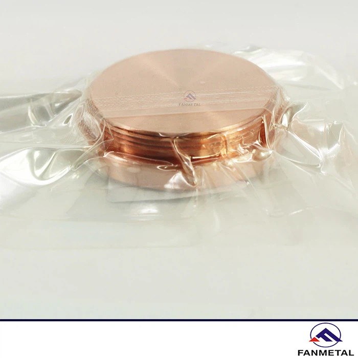
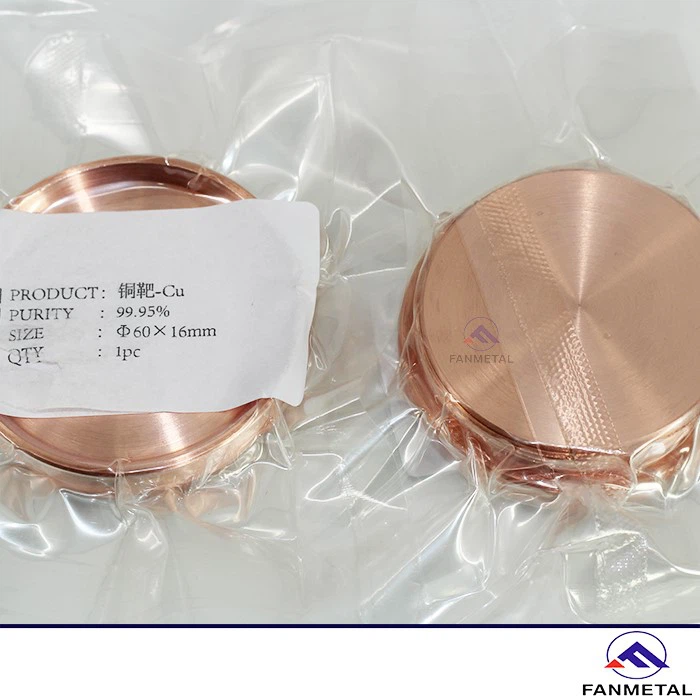
Copper sputtering targets occupy a core position in many fields such as semiconductor manufacturing, the photovoltaic industry, display technology, and so on, with their excellent physical and chemical properties. As the key raw material for IC and film production, the quality of copper sputtering targets directly affects the performance and reliability of the final product.
Production process
Purity is one of the key factors affecting Copper sputtering targets' performance, and copper is usually required to be 99.99% pure or higher. The selected high-purity copper material is melted in a controlled environment to avoid the introduction of impurities. The molten copper is then poured into a pre-prepared mold and cooled to form. This stage controls the cooling speed and direction of the copper to avoid internal defects. Then, through the rolling process, the cast copper billet is processed into a plate of specific thickness. During the rolling process, the pressure and speed are precisely controlled to ensure the uniformity and flatness of the material. Finally, according to the specific needs of customers, the rolled copper plate is cut, punched, and other mechanical processing is performed to make a specific shape and size of the target material.
Excellent features of Copper sputtering targets
(1) High purity: Copper sputtering targets are usually required to have very high purity, generally 99.99% or higher, which ensures that a high-quality coating can be obtained during the film deposition process, reducing the risk of impurity introduction. It is important to improve the performance of semiconductor devices and photovoltaic modules.
(2) Excellent electrical conductivity: Copper is an excellent conductive material; its target form maintains a high conductivity, which is particularly critical for the manufacture of conductive paths in electronic devices.
(3) High thermal conductivity: ensures that heat can be effectively transferred during use, reduces energy consumption, and improves production efficiency and product quality.
(4) Good mechanical properties: with good ductility and toughness, easy to process into different shapes and sizes to meet the needs of diverse applications.
(5) Long service life: Its good mechanical properties and surface treatment technology give it a higher utilization rate and less maintenance needs in the manufacturing process, thereby improving production efficiency.
(6) Strong adaptability: The excellent physical and chemical properties of Copper Target Back Plate make it widely applicable to a variety of high-tech manufacturing fields, such as integrated circuits, photovoltaic power generation, and display technology.
Application field
(1) Semiconductor industry
Integrated circuit manufacturing: Copper's high conductivity makes it an ideal material for connecting transistors, improving the performance and energy efficiency of ICs.
Thin film deposition technology: Through physical vapor deposition (PVD) and other technologies, the use of copper target back plates to form a thin film on the substrate; these films can be used to manufacture circuit boards and chips.
(2) Photovoltaic industry
Copper sputtering targets play a key role in the process of making thin films for solar cells, especially in the production of copper indium gallium selenium (CIGS) solar cells. Copper's excellent conductive properties and chemical stability make it an important part of this type of battery material, which greatly improves the efficiency of solar energy conversion.
(3) Electronic display technology
Liquid crystal display (LCD): Copper sputtering target is often used to produce thin-film circuits in LCDS, and its high conductivity ensures that signals are transmitted quickly and accurately, improving display quality and device response speed.
Organic light-emitting diode (OLED): In OLED display technology, the high electrical conductivity and good heat conduction properties of copper help to improve the light efficiency and life of OLED displays.